- 您现在的位置:买卖IC网 > Sheet目录395 > AS3930-BTST (ams)IC ASK RECEIVER 1CH LP 16-TSSOP
AS3930
Datasheet - A b s o l u t e M a x i m u m R a t i n g s
5 Absolute Maximum Ratings
Stresses beyond those listed in Table 3 may cause permanent damage to the device. These are stress ratings only. Functional operation of the
device at these or any other conditions beyond those indicated in Electrical Characteristics on page 7 is not implied. Exposure to absolute
maximum rating conditions for extended periods may affect device reliability.
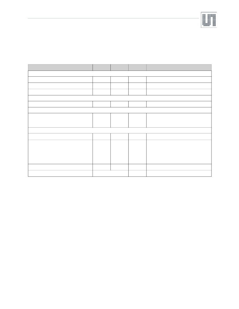
Table 3. Absolute Maximum Ratings
Parameter
Min
Max
Units
Notes
Electrical Parameters
DC supply voltage (V DD )
Input pin voltage (V IN )
-0.5
-0.5
5
5
V
V
Input current (latch up immunity) (I SOURCE )
-100
100
mA
Norm: Jedec 78
Electrostatic Discharge
Electrostatic discharge (ESD)
±2
kV
Norm: MIL 883 E method 3015 (HBM)
Continuous Power Dissipation
Total power dissipation
(all supplies and outputs)
(P t )
Temperature Ranges and Storage Conditions
0.07
mW
Storage temperature (T strg )
-65
150
oC
Package body temperature (T body )
260
oC
Norm: IPC/JEDEC J-STD-020
The reflow peak soldering temperature (body
temperature) is specified according IPC/JEDEC
J-STD-020 “Moisture/Reflow Sensitivity
Classification for Non-hermetic Solid State
Surface Mount Devices”.
Humidity non-condensing
Moisture sensitivity level (MSL)
www.ams.com/LF-Receiver/AS3930
5
3
85
Revision 1.5
%
Represents a maximum floor time of 168h
6 - 32
发布紧急采购,3分钟左右您将得到回复。
相关PDF资料
AS3931-ZTSU
IC ASK RECEIVER LF 3CH 16-TSSOP
AS3932-BTST
IC RF PROGRAM 16-TSSOP
AS500106
TLAPS MAGNET CARRIER
AS5263-HQFT-500
IC ENCODER ROTARY 12BIT 32-QFN
AT 150 B420L
SENSOR CURRENT 150A 30V MOD
AT 150 B5
SENSOR CURRENT 150A MOD
AT 20 B10
SENSOR CURRENT 20A MOD
AT-7666A
SENSOR AMORPHOUS 146X167.5X0.3
相关代理商/技术参数
AS3930-DB
制造商:ams 功能描述:AS3930 Demo Board
AS3931
制造商:AMS 功能描述:AS Series 19 to 150 kHz Surface Mount 3D Wakeup Receiver - TSSOP-16
AS3931 DB
制造商:AMS 功能描述:BOARD DEMO FOR AS3931 制造商:AMS 功能描述:Demoboard for AS3931 3D Low Power Wakeup Receiver
AS39310FLF
制造商:TT Electronics / IRC 功能描述:AS39310FLF
AS39310HLF
制造商:TT Electronics / IRC 功能描述:AS39310HLF
AS39310JLF
制造商:TT Electronics / IRC 功能描述:AS39310JLF
AS39311FLF
制造商:TT Electronics / IRC 功能描述:AS39311FLF
AS39311HLF
制造商:TT Electronics / IRC 功能描述:AS39311HLF
